Building 3D Structures from a 2D Template
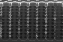
Deep below the silicon surface, the SPRIE method produces regular structures in the micrometer range that refract light. (Photo: KIT/CFN)<br>
In modern telecommunications, light carries digital information over kilometers within seconds. Adapted optical materials control the light signals. In the AFM journal, researchers from Berlin, Louvain, and from Karlsruhe Institute of Technology present a method to produce photonic crystals. Their optical properties are adjusted by structures of micrometer size. The method is rapid, cheap, and simple and partly uses the self-organization principle (DOI: 10.1002/adfm.201201138).
“Optical properties of materials can be influenced decisively by specific structurization,” explains Andreas Frölich from Karlsruhe Institute of Technology. Silicon is used in components, e.g. filters or deflectors, for telecommunications. So far, however, all these components have been flat, i.e. two-dimensional. Entirely novel concepts might be feasible using three-dimensional components. The expenditure required to structure the silicon is very high. The structure has to be very regular in all three spatial directions and details are to have the size of about one micrometer, which corresponds to one hundredth of the thickness of a hair.
“Our new SPRIE fabrication methods uses established technologies, such as etching and innovative methods like self-organization and combines them in a very creative manner,” says Martin Wegener, Professor of the Institute of Applied Physics and Institute of Nanotechnology of KIT and coordinator of the DFG Center for Functional Nanostructures (CFN). The SPRIE method is applied to structure silicon on large areas in a simple and three-dimensional manner. First, a solution with micrometer-sized spheres of polystyrene is applied to the silicon surface. After drying, these spheres automatically form in a dense monolayer on the silicon. Upon metal coating and the removal of the spheres, a honeycomb etching mask remains on the silicon surface.
“This etching mask is our two-dimensional template for the construction of the three-dimensional structure,” says Frölich. The free areas are removed by etching with a reactive plasma gas. An electric field is applied to make the gas particles etch into the depth only or homogeneously in all directions.” In addition, we can specifically passivate the walls of the hole, which means that it is protected from further etching by a polymer layer.”
Repeated etching and passivation makes the holes of the etching mask grow into the depth. With up to 10 micrometers, their depth exceeds their width by a factor of more than 10. The process steps and the electric field are adjusted precisely to control the structure of the walls. Instead of a simple hole with vertical smooth walls, every etching step produces a spherical depression with a curved surface. This curvature is the basis for the regular repeating structures of novel waveguides. “Optical telecommunication takes place at a wavelength of 1.5 µm. With our etching method, we produce a corrugated structure in the micrometer range along the wall.” The field at closely adjacent and very deep, structured holes acts like a regular crystal that refracts in the desired manner.
The SPRIE (Sequential Passivation and Reactive Ion Etching) method can produce a three-dimensional photonic crystal within a few minutes, as it is based on conventional industrial processes. In principle, a three-dimensional structure can be generated in silicon using a freely choosable mask. This opens up new possibilities for meeting the requirements made on optical components in telecommunications.
Different designs of photonic crystals are available. Some are applied as waveguides with very small curvature radii and small losses or as extremely small-band optical filters and multiplexers. In few decades, computers working with light instead of electricity might be feasible. Apart from KIT, the Belgian Université catholique de Louvain and Humboldt University, Berlin, were involved in the development.
The publication in the Advanced Functional Materials journal:
http://onlinelibrary.wiley.com/journal/10.1002/%28ISSN%291616-3028
Karlsruhe Institute of Technology (KIT) is a public corporation according to the legislation of the state of Baden-Württemberg. It fulfills the mission of a university and the mission of a national research center of the Helmholtz Association. KIT focuses on a knowledge triangle that links the tasks of research, teaching, and innovation.
kes, 05.10.2012
For further information, please contact:
Kosta Schinarakis
PKM, Themenscout
Tel.: +49 721 608-41956
Fax: +49 721 608-43568
E-Mail:schinarakis@kit.edu
Media Contact
All latest news from the category: Materials Sciences
Materials management deals with the research, development, manufacturing and processing of raw and industrial materials. Key aspects here are biological and medical issues, which play an increasingly important role in this field.
innovations-report offers in-depth articles related to the development and application of materials and the structure and properties of new materials.


Newest articles
Decisive breakthrough for battery production
Storing and utilising energy with innovative sulphur-based cathodes. HU research team develops foundations for sustainable battery technology Electric vehicles and portable electronic devices such as laptops and mobile phones are…

Superradiant atoms could push the boundaries of how precisely time can be measured
Superradiant atoms can help us measure time more precisely than ever. In a new study, researchers from the University of Copenhagen present a new method for measuring the time interval,…

Ion thermoelectric conversion devices for near room temperature
The electrode sheet of the thermoelectric device consists of ionic hydrogel, which is sandwiched between the electrodes to form, and the Prussian blue on the electrode undergoes a redox reaction…

