Power Electronics: Ceramic Embedding Gives a Boost to Wide Bandgap Semiconductor Devices
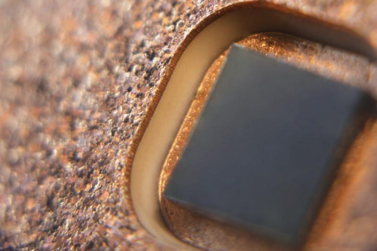
Close-up view of a wide-bandgap device embedded by the Ceramic Embedding technology. Fraunhofer IISB
Ongoing miniaturization, 3D integration, and extreme environmental conditions impose major challenges to future power devices, modules, and systems, which are expected to provide excellent performance, high reliability, and long lifetime. Low cost is a key, enabled by high temperature.
This implies small chip size and low cooling effort. In this respect, the applicability of established packaging technologies, e.g., based on PCBs (Printed Circuit Boards), is limited as they do not afford sufficient thermal stability or current carrying capability.
As a remedy, a novel packaging concept was developed at Fraunhofer IISB in Erlangen, which is based on the embedding of power semiconductors in ceramic circuit carriers.
This prepares the ground for an extensive and more economical use of wide-bandgap semiconductors such as SiC (silicon carbide). SiC devices offer a vast potential for the growing market of power electronics.
They allow the switching of very high currents and voltages in compact, miniaturized systems and thus are a key enabler for the development of highly efficient and intelligent solutions for mobility, industrial applications, and energy technology. With the new approach for packaging and circuit carriers, the existing physical constraints, such as limited operation temperature or undesired parasitic inductances, can be enhanced.
With the new technology – called Ceramic Embedding – the power devices are placed inside a special prepared direct bonded copper (DBC) substrate by suitable die bonding techniques such as soldering or silver sintering. Subsequently, all gaps are filled with a high-temperature potting material. The resulting prepackage is forming an easy-to-use power electronics building block.
The concept allows a high copper layer thickness, which paves the way for a considerable current carrying capacity. A big benefit is the high electrical and thermal contact area. The semiconductor’s top and bottom side have ideal interconnections offering the full performance of the tiny WBG devices.
Different types of ceramic material are applicable such as alumina, aluminum nitride or silicon nitride. The choice depends on the individual requirements for optimizing the thermal management, mechanical properties, and cost.
For generating the cavities and trenches, subtractive manufacturing methods are used. The vias for the electrical contacts are drilled with a laser process. Then they are filled with silver sintering material or similar conductive materials. The vias allow the realization of multi-layer ceramic substrate stacks, which are of special advantage for low-inductance commutation cells.
Fraunhofer IISB is continuing its intensive research on Ceramic Embedding and the necessary manufacturing process technologies to exploit the full potential of wide-bandgap semiconductor devices in power electronics. The target is to bring the promising packaging technology to industrial production.
Power modules based on the Ceramic Embedding technology can be discovered on May 7-9, 2019, at the PCIM Europe exhibition in Nuremberg, booth no. 6-438.
Andreas Schletz
Fraunhofer IISB, Schottkystrasse 10, 91058 Erlangen, Germany
Tel. +49 9131 761 187 | andreas.schletz@iisb.fraunhofer.de
www.iisb.fraunhofer.de
https://www.iisb.fraunhofer.de/ Homepage Fraunhofer IISB
https://www.iisb.fraunhofer.de/presse Pressemitteilungen Fraunhofer IISB
Media Contact
All latest news from the category: Trade Fair News


Newest articles

Zap Energy achieves 37-million-degree temperatures in a compact device
New publication reports record electron temperatures for a small-scale, sheared-flow-stabilized Z-pinch fusion device. In the nine decades since humans first produced fusion reactions, only a few fusion technologies have demonstrated…
Innovative microscopy demystifies metabolism of Alzheimer’s
Researchers at UC San Diego have deployed state-of-the art imaging techniques to discover the metabolism driving Alzheimer’s disease; results suggest new treatment strategies. Alzheimer’s disease causes significant problems with memory,…

A cause of immunodeficiency identified
After stroke and heart attack: Every year, between 250,000 and 300,000 people in Germany suffer from a stroke or heart attack. These patients suffer immune disturbances and are very frequently…

