Plumbing the depths: Defect distribution in ion-implanted SiC diodes
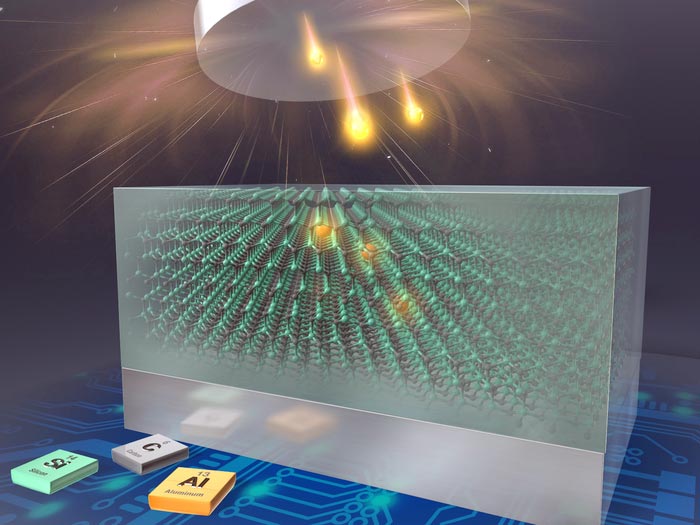
Ion implantation is a low-temperature method of ‘doping’ semiconductor devices in which high energy charged particles (ions) are accelerated towards a semiconductor, causing the ions to penetrate into and settle in the semiconductor’s layers.
Photo courtesy: Masashi Kato from Nagoya Institute of Technology
Researchers reveal that aluminum implantation doping in p-type bipolar semiconductors creates defects many layers deeper than the implantation site.
Silicon carbide (SiC) unipolar semiconductors are in wide commercial use, but their operations are limited by a trade-off relationship between breakdown voltage and specific resistance of the drift layer, or specific on-resistance. Including a super junction structure, which refers to an arrangement of n and p layers in trenches in the drift layer, or enabling bipolar operation in the device provides a way to overcome this unipolar limit. Bipolar operation brings about a large decrease in on-resistance by inducing a conductivity modulation in the drift layer. But bipolar operation is not without its disadvantages. Conduction and switching losses in bipolar devices need to be carefully balanced.
P-type contact layers in semiconductors are generally formed via aluminum (Al) doping. Al doping can be achieved in two ways – epitaxial or ion implantation. Epitaxial growth involves the layer by layer deposition of semiconductor materials on a substrate, whereas ion implantation entails bombarding the semiconductor layers with high energy charged particles. But ion implantation leads to the formation of defects deep in the semiconductor layers, which could have a critical effect on conductivity modulation.
In a recent study published in Physica Status Solidi (b), researchers from Japan investigated the depth distribution of defects in SiC bipolar diodes that were formed by Al doping. “Our findings will help with the optimum design of SiC power devices, which will soon be employed in electric vehicles, trains etc. These results will ultimately help improve the performance, as well as the size and energy consumption of traction systems in vehicles and trains,” says Associate Professor Dr. Masashi Kato of Nagoya Institute of Technology, who led the study.
To study the depth distribution of defects, the research team fabricated two SiC PiN diodes with Al doped p-layers, one through epitaxial growth and the other through ion implantation. They then studied the distribution of defects in both diodes using conventional ‘deep level transient spectroscopy’ (DLTS) and characterized its properties using cathodoluminescence (CL). They found that p-type layer deposition by epitaxial growth did not cause damage in the adjacent n-type layers, but that the growth showed slight instability that led to the formation of deep level defects. The specific on-resistance of this diode was also low, thanks to the effects of conductivity modulation.
For the diode formed by ion implantation, however, the researchers found that Al doping achieved a high specific on-resistance without influencing conductivity modulation. Moreover, the researchers observed that the defects in the semiconductor device penetrated to a minimum of 20 µm from the implantation region. “Our study shows that the ion implantation in SiC bipolar devices need to be processed at least 20 µm away from the active regions,” explains Dr. Kato.
The low power consumption of SiC power devices mean that they will be essential in the future as climate change increases and the fossil fuel energy crisis worsens. Improving semiconductor technology rapidly so that it can take its rightful place on the world stage is of paramount importance. With strong results like this to inform future research and manufacturing, we may realize this future sooner than expected!
Journal: physica status solidi (b)
DOI: 10.1002/pssb.202100419
Method of Research: Experimental study
Subject of Research: Not applicable
Article Title: Depth distribution of defects in SiC PiN diodes formed using ion implantation or epitaxial growth
Article Publication Date: 20-Oct-2021
COI Statement: None
Media Contact
Azusa Yabugami
Nagoya Institute of Technology
yabugami.azusa@nitech.ac.jp
Office: 81-527-355-091
Original Source
All latest news from the category: Power and Electrical Engineering
This topic covers issues related to energy generation, conversion, transportation and consumption and how the industry is addressing the challenge of energy efficiency in general.
innovations-report provides in-depth and informative reports and articles on subjects ranging from wind energy, fuel cell technology, solar energy, geothermal energy, petroleum, gas, nuclear engineering, alternative energy and energy efficiency to fusion, hydrogen and superconductor technologies.


Newest articles
Solving the riddle of the sphingolipids in coronary artery disease
Weill Cornell Medicine investigators have uncovered a way to unleash in blood vessels the protective effects of a type of fat-related molecule known as a sphingolipid, suggesting a promising new…
Rocks with the oldest evidence yet of Earth’s magnetic field
The 3.7 billion-year-old rocks may extend the magnetic field’s age by 200 million years. Geologists at MIT and Oxford University have uncovered ancient rocks in Greenland that bear the oldest…
Mini-colons revolutionize colorectal cancer research
As our battle against cancer rages on, the quest for more sophisticated and realistic models to study tumor development has never been more critical. Until now, research has relied on…

