Perovskite edges can be tuned for optoelectronic performance
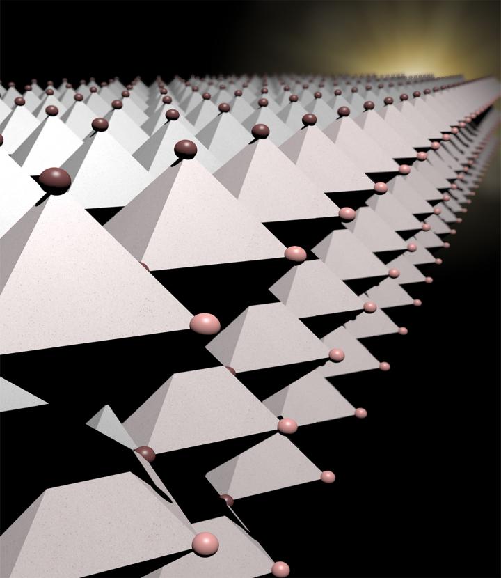
Scientists at Los Alamos National Laboratory and their research partners are creating innovative 2-D layered hybrid perovskites that allow greater freedom in designing and fabricating efficient optoelectronic devices. Credit: Los Alamos National Laboratory
In the eternal search for next generation high-efficiency solar cells and LEDs, scientists at Los Alamos National Laboratory and their partners are creating innovative 2D layered hybrid perovskites that allow greater freedom in designing and fabricating efficient optoelectronic devices. Industrial and consumer applications could include low cost solar cells, LEDs, laser diodes, detectors, and other nano-optoelectronic devices.
“Our material is a layered compound, meaning it is a stack of 2D layers of perovskites with nanometer thickness (like a stack of sheets), and the 2D perovskite layers are separated by thin organic layers,” said Jean-Christophe Blancon, lead author on a paper out today in the journal Science's First Release distribution. “This work could overturn conventional wisdom on the limitations of device designs based on layered perovskites.”
The 2D, near-single-crystalline “Ruddlesden-Popper” thin films have an out-of-plane orientation so that uninhibited charge transport occurs through the perovskite layers in planar devices. At the edges of the perovskite layers, the new research discovered “layer-edge-states,” which are key to both high efficiency of solar cells (>12 percent) and high fluorescence efficiency (a few tens of percent) for LEDs. The spontaneous conversion of excitons (bound electron-hole pairs) to free carriers via these layer-edge states appears to be the key to improving the photovoltaic and light-emitting thin-film layered materials.
The team investigated both photophysical and optoelectronic properties of phase-pure homogenous 2D perovskites. They were able to show that thin films have an intrinsic mechanism for dissociation of the strongly bound electron-hole pairs (excitons) to long-lived free-carriers provided by lower energy states at the edges of the layered perovskites.
Moreover, once carriers are trapped in these edge states, they remain protected and do not lose their energy via non-radiative processes. They can contribute to photocurrent in a photovoltaic (PV) device or radiatively recombine efficiently for light-emission applications. “These materials are quantum hybrid materials, possessing physical properties of both organic semiconductors and inorganic semiconducting quantum wells. We are just beginning to understand the interplay of the organic and inorganic components in 2D perovskites and this result underpins how unique properties can arise from competing physical properties,” said Jared Crochet of the Physical Chemistry and Applied Spectroscopy group at Los Alamos.
“These results address a long-standing problem not just for the perovskite family, but relevant to a large group of materials where edges and surface states generally degrade the optoelectronic properties, which can now be chemically designed and engineered to achieve efficient flow of charge and energy leading to high-efficiency optoelectronic devices,” said Aditya Mohite, who leads the perovskite program in the Material Synthesis and Integrated devices group at Los Alamos.
“The 2D hybrid perovskites continue to surprise. When we first designed these materials we were hoping that high quality samples of them would exhibit novel optoelectronic properties,” said co-author Mercouri Kanatzidis of Northwestern University. “Well, they have done so and then some. They have exceeded our expectations and are proving to be truly amazing systems. We have only scratched the surface of what is there–sorry for the pun–in this 2D family and we anticipate continued excitement going forward.”
###
The paper: “Extremely efficient internal exciton dissociation through edge-states in layered 2D perovskites,” J.-C. Blancon, W. Nie, S. Tretiak, J. J. Crochet and A. D. Mohite of Los Alamos National Laboratory; H. Tsai and P. M. Ajayan of Rice University, Houston, Texas; C. C. Stoumpos, C. M. M. Soe, and M. G. Kanatzidis of Northwestern University, Evanston, Illinois; L. Pedesseau and J. Even of Fonctions Optiques pour les Technologies de l'Information (FOTON), INSA de Rennes, France; C. Katan and M. Kepenekian of Institut des Sciences Chimiques de Rennes (ISCR), Université de Rennes, France; K. Appavoo and M. Y. Sfeir of Brookhaven National Laboratory, Upton, New York.. This paper will be published online by the journal Science on Thursday, March 9, 2017.
http://science.
Funding: The work at Los Alamos National Laboratory was supported by the Laboratory Directed Research and Development program and was partially performed at the Center for Nonlinear Studies. The work was conducted, in part, at the Center for Integrated Nanotechnologies (CINT), a U.S. Department of Energy, Office of Science user facility. Work at Northwestern University was supported by grant SC0012541 from the U.S. Department of Energy, Office of Science. The work in France was supported by Cellule Energie du CNRS (SOLHYBTRANS Project) and University of Rennes 1 (Action Incitative, Défis Scientifique Emergents 2015). This research used resources of the Center for Functional Nanomaterials, which is a U.S. DOE Office of Science Facility, at Brookhaven National Laboratory under Contract No. DE-SC0012704.
About Los Alamos National Laboratory
Los Alamos National Laboratory, a multidisciplinary research institution engaged in strategic science on behalf of national security, is operated by Los Alamos National Security, LLC, a team composed of Bechtel National, the University of California, BWX Technologies, Inc. and URS Corporation for the Department of Energy's National Nuclear Security Administration.
Los Alamos enhances national security by ensuring the safety and reliability of the U.S. nuclear stockpile, developing technologies to reduce threats from weapons of mass destruction, and solving problems related to energy, environment, infrastructure, health and global security concerns.
Media Contact
All latest news from the category: Materials Sciences
Materials management deals with the research, development, manufacturing and processing of raw and industrial materials. Key aspects here are biological and medical issues, which play an increasingly important role in this field.
innovations-report offers in-depth articles related to the development and application of materials and the structure and properties of new materials.


Newest articles

High-energy-density aqueous battery based on halogen multi-electron transfer
Traditional non-aqueous lithium-ion batteries have a high energy density, but their safety is compromised due to the flammable organic electrolytes they utilize. Aqueous batteries use water as the solvent for…

First-ever combined heart pump and pig kidney transplant
…gives new hope to patient with terminal illness. Surgeons at NYU Langone Health performed the first-ever combined mechanical heart pump and gene-edited pig kidney transplant surgery in a 54-year-old woman…

Biophysics: Testing how well biomarkers work
LMU researchers have developed a method to determine how reliably target proteins can be labeled using super-resolution fluorescence microscopy. Modern microscopy techniques make it possible to examine the inner workings…

