Electron Spins Separated on a Semiconductor Surface
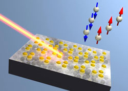
Würzburg physicists have determined the spin architecture of a semiconductor surface. For this purpose, electrons were displaced from the material by means of photo-excitation so that their spin orientation could be measured.<br>Graphics: Philipp Höpfner<br>
In a recent publication, physicists of the University of Würzburg describe the spin architecture of an ultra-thin metal layer on a semiconductor for the first time. This represents yet another step towards high-performing super computers.
The development of significantly faster computers might be feasible if the spin of electrons could be used as information carrier in data processing.
What is this electron spin? The spin gives the electron magnetic properties in addition to its electric charge. “You can imagine each electron as carrying a tiny elementary magnet, just like a compass needle,” explains the Würzburg physicist, Jörg Schäfer.
In order to use the electron spin in electronics, thus implementing spintronics, it would be required to arrange the electrons flowing in a semiconductor chip by their spin state, i.e. to align their spin orientation. These elementary magnetic needles would have to keep this spin formation when traveling through the electronic device as so-called spin currents.
Trick allows spin separation without magnetic fields
It has been known for a long time that the spins can be manipulated by magnetic fields. However, this is not at all practicable for electronic applications. Therefore, the solid-state physicists devised an ingenious trick: An ultra-thin metal layer with a thickness of only one atom is vapor-deposited on a semi-conducting solid material. In this system, the electrons spontaneously sort themselves into two groups with opposite magnet needle orientation.
This effect is the more pronounced, the heavier the respective metal atoms are. “We wanted to produce and further examine this automatic spin separation in a model experiment,” explains Professor Ralph Claessen. The Würzburg physicists decided to use gold as a particularly heavy metal, which they vapor-deposited in a wafer-thin layer on a semiconductor substrate consisting of Germanium.
Close interaction between theory and experiment
The experimental findings on the spin pattern correspond very accurately to the predictions developed by the Würzburg theoretical physicists working with Professor Werner Hanke. “We can create a mathematical model of the spin structure in the semiconductor, enabling us to make very accurate practical predictions with state-of-the-art computers,” Hanke explains.
The spin pattern can be experimentally verified by means of photoemission spectroscopy. The relevant measurements were conducted at the Paul Scherrer Institute in Switzerland. In these measurements, the semiconductor surface with the gold layer is subjected to the particularly intensive X-ray radiation of a synchrotron. This causes electrons to get loose and fly out of the sample at various angles – depending on their spin – which can be spotted by detectors.
Two spin orientations clearly identified for the first time
“We observed a marked splitting of the spins into two groups with opposite orientation of the magnet needles and a special spin pattern,” says Jörg Schäfer. Thus, all spins point out of the surface or into it. “The merit of this collaboration in the fields of theoretical and experimental physics lies in the fact that the three-dimensional spin pattern has been clarified for the first time,” says Ralph Claessen. In particular, the results clearly show that the separation of the conduction electrons by their spin works well. Thus, they can be sent separately on their journey through the metal. This is new and important fundamental knowledge for spintronics.
The editor of the scientific journal “Physical Review Letters” was outright enthusiastic about these findings: The successful research from Würzburg is specially recommended for perusal to the knowledgeable readers of the journal as “Editor's Suggestion”.
Study conducted within a DFG research group
The publication arose from Würzburg research group 1162, which has been funded by the German Research Foundation (DFG) with about three million euros since 2009. The group examines electronic quantum effects in nanostructures; Ralph Claessen is its spokesperson.
“Three-Dimensional Spin Rotations at the Fermi Surface of a Strongly Spin-Orbit Coupled Surface System”, P. Höpfner, J. Schäfer, A. Fleszar, J. H. Dil, B. Slomski, F. Meier, C. Loho, C. Blumenstein, L. Patthey, W. Hanke, and R. Claessen, Physical Review Letters 108, 186801 (2012), DOI 10.1103/PhysRevLett.108.186801
Contact person
Prof. Dr. Ralph Claessen, Institute of Physics of the University of Würzburg, T +49 (0)931 31-85732, claessen@physik.uni-wuerzburg.de
Media Contact
More Information:
http://www.uni-wuerzburg.deAll latest news from the category: Physics and Astronomy
This area deals with the fundamental laws and building blocks of nature and how they interact, the properties and the behavior of matter, and research into space and time and their structures.
innovations-report provides in-depth reports and articles on subjects such as astrophysics, laser technologies, nuclear, quantum, particle and solid-state physics, nanotechnologies, planetary research and findings (Mars, Venus) and developments related to the Hubble Telescope.


Newest articles

Zap Energy achieves 37-million-degree temperatures in a compact device
New publication reports record electron temperatures for a small-scale, sheared-flow-stabilized Z-pinch fusion device. In the nine decades since humans first produced fusion reactions, only a few fusion technologies have demonstrated…
Innovative microscopy demystifies metabolism of Alzheimer’s
Researchers at UC San Diego have deployed state-of-the art imaging techniques to discover the metabolism driving Alzheimer’s disease; results suggest new treatment strategies. Alzheimer’s disease causes significant problems with memory,…
A cause of immunodeficiency identified
After stroke and heart attack: Every year, between 250,000 and 300,000 people in Germany suffer from a stroke or heart attack. These patients suffer immune disturbances and are very frequently…

