Electron Beam Patterning for high-resolution full-color OLED displays
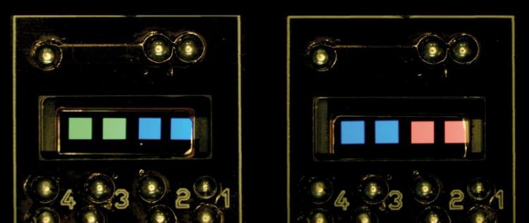
Test OLEDs on silicon substrate patterned by electron beam processing © Fraunhofer FEP | Picture in printable resolution: www.fep.fraunhofer.de/press
The average smartphone user looks at a display about 88 times a day, not counting viewing smaller smart watches or other displays. Displays of all kinds have become ubiquitous and will soon be irreplaceable in everyday life.
If you turn your attention to the world of OLED microdisplays, you will quickly find yourself immersed in data glasses for current and future Virtual Reality (VR) and Augmented Reality (AR) applications, the core of which is the microdisplay. Since the Pokémon Go mania everyone has an idea of what AR means – additional interactive information is being interwoven into the real world.
In addition to industrial use in Production 4.0 programs and products, its use in medical technology and in electronic entertainment, AR and VR applications have also been established for years in advertising and the education sector. The days of bulky audio guides in museums could soon be over.
And not only as a result of previous solutions like tablets and smartphones. Lightweight head-up displays can turn exhibitions into great learning worlds by integrating film scenes, audio, and interaction with the visitor to make a museum experience more memorable.
Thanks to the shallow overall depth that results from the self-luminous properties of OLEDs and their excellent contrast ratios, manufacturers are increasingly turning to OLED microdisplays for AR/VR glasses. Fraunhofer FEP has been continuously immersed in the advanced development of this technology for several years.
Nevertheless, there are still some technological challenges that need to be mastered in order to exploit the full potential of OLED technology for use in consumer-ready data glasses and other AR/VR applications. Very high brightness and efficiency, good yields for large chip areas, curved surfaces, integrated eye tracking, and transparent substrates are some of the tasks still on the researchers' agenda.
Currently, OLED technology faces the hurdle that full-color displays can only be realized by using color filters or shadow masks, which limit OLED efficiency and resolution. Researchers are working intensely on new approaches to fabricate microdisplays characterized by high resolution while at the same time offering high efficiency and long operating life time.
The patterning of the organic layers of OLEDs is one of the greatest challenges, since conventional methods such as photolithography cannot be utilized with organic semiconductor materials. The use of electron beam technology for microstructuring was successfully demonstrated at the Fraunhofer FEP two years ago. Using its patented process, FEP was able to modify the emission of an OLED through the existing encapsulation layer to create any feature imaginable and even produce high-resolution grayscale images.
Further development of the electron beam process has now achieved full-color OLED without using color filters or shadow masks. To create red, green, and blue pixels, an organic layer of the OLED itself is ablated by a thermal electron beam process. This patterning causes a change to the thickness of the layer stack, which makes the emission of different colors possible.
This is the first major step towards the development of full-color displays without the use of restrictive color filters in the process. Elisabeth Bodenstein, developer in the Fraunhofer FEP project team, explains the advantages: “With our electron-beam process it is possible to thermally structure even these sensitive organic materials without damaging the underlying layer.”
The results were obtained by simulating and initially estimating the HTL (hole transport layer) thicknesses that are produced by the electron beam. The researchers actually achieved the decoupling of red, green, and blue emissions from the white OLED. Following proof of concept at Fraunhofer FEP, these colors were demonstrated on the first test substrates, exhibiting comparable OLED performance.
In addition to using this new process for OLEDs, electron beam processing can also be used for other applications in organic electronics and inorganic layers. Moreover, the electron-beam patterning process is very adaptable and can also be employed in the areas of photovoltaics, MEMS, and thin-film technology.
Now Fraunhofer FEP scientists are approaching the next milestones, having completed the promising preparatory work. The main goal in the coming years is to use this new method in jointly developing fabrication of OLED microdisplays with partners and establish it in the industry through licensing. To do this, the features will be further miniaturized and the process optimized by working together with interested partners from industry.
The next step planned is to integrate the micropatterning into existing processes in order to gain further know-how jointly with industrial partners. This should enable future transfer of the test results into an existing process line to be worked out in order to facilitate establishing the technology at the industrial level at a later date.
In parallel, the scientists are also planning an enhanced simulation of OLEDs. The OLED color spectrum will be broadened by suitably modifying the materials and layer thicknesses. In this way, the prospective incorporation the displays in data glasses for special applications such as in industrial manufacturing and medicine should be opened up with the new process.
The development of the new technology is the result of a project funded by the Fraunhofer-Gesellschaft. Now the scientists are ready for specific advanced development of the technology through partnerships and joint projects with display, plant, material and system manufacturers. The results with first colored OLEDs will also be presented at the Fraunhofer FEP booth no. 50 and in poster session III during the International Meeting on Information Display – IMID 2018 in Busan, South Korea, August 29-31, 2018.
Fraunhofer FEP at the IMID 2018
Busan Exhibition and Convention Center (BEXCO), Busan, South Korea
Hall 2B, Booth No. 50
Conference Presentation:
Session 05: Near-Eye Display for AR/VR/MR
Wednesday, August 29, 2018, 9:00-10:20 a.m.
Room E (311~312)
Invited Talk: Advanced OLED Microdisplays for Virtual and Augmented-Reality Applications, Dr. Uwe Vogel, Fraunhofer FEP
Poster:
Session 05: Poster Session III
Friday, August 31, 2018, 2:00 – 3:30 p.m.
Room 2B Hall (Room 1F)
Paper No. L_10_1003: Electron Beam Patterning for Realization of RGB Microcavity OLEDs
Authors: Elisabeth Bodenstein, Matthias Schober, Stefan Saager, Christoph Metzner, Uwe Vogel; Fraunhofer FEP, Germany
The world's first experiments on advanced micropatterning of OLEDs with electron beams at Fraunhofer FEP and their results were recently published in the paper “Realization of RGB colors from top-emitting white OLED by electron-beam patterning” in the Journal of the Society for Information Display (http://s.fhg.de/kei).
Press contact:
Fraunhofer Institute for Organic Electronics, Electron Beam and Plasma Technology FEP
Winterbergstraße 28 | 01277 Dresden, Germany | www.fep.fraunhofer.de
Head of Marketing: Ines Schedwill | Phone +49 351 8823-238 |ines.schedwill@fep.fraunhofer.de
Head of Corporate Communications: Annett Arnold, M.Sc. | Phone +49 351 2586-333 | annett.arnold@fep.fraunhofer.de
Media Contact
More Information:
http://www.fep.fraunhofer.de/All latest news from the category: Power and Electrical Engineering
This topic covers issues related to energy generation, conversion, transportation and consumption and how the industry is addressing the challenge of energy efficiency in general.
innovations-report provides in-depth and informative reports and articles on subjects ranging from wind energy, fuel cell technology, solar energy, geothermal energy, petroleum, gas, nuclear engineering, alternative energy and energy efficiency to fusion, hydrogen and superconductor technologies.


Newest articles
Bringing bio-inspired robots to life
Nebraska researcher Eric Markvicka gets NSF CAREER Award to pursue manufacture of novel materials for soft robotics and stretchable electronics. Engineers are increasingly eager to develop robots that mimic the…

Bella moths use poison to attract mates
Scientists are closer to finding out how. Pyrrolizidine alkaloids are as bitter and toxic as they are hard to pronounce. They’re produced by several different types of plants and are…
AI tool creates ‘synthetic’ images of cells
…for enhanced microscopy analysis. Observing individual cells through microscopes can reveal a range of important cell biological phenomena that frequently play a role in human diseases, but the process of…

