Custom-made photonic components
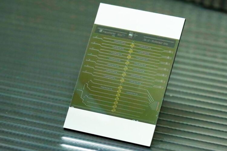
Biosensor chip from Fraunhofer IPMS.
©Fraunhofer IPMS
Innovative, customized, and sustainable – these are the keywords for the numerous research projects of the Fraunhofer IPMS. At one of the leading conferences and trade fairs for photonics – SPIE Photonics West in San Francisco from January 27 to February 1, 2024 – the institute will present developments and advances in areas such as micro-optics, MEMS-based light modulators and biophotonics.
The Fraunhofer Institute for Photonic Microsystems IPMS is one of the leading research institutes for the development and production of electronic, micromechanical, and optical components and their integration into intelligent systems. With innovative micro-electro-mechanical systems (MEMS) and micro-opto-electro-mechanical systems (MOEMS), the institute opens up new applications through improved properties and additional functions. These include smaller dimensions, higher energy efficiency and increased performance. The institute will present some of its many research results at the photonics tech event SPIE Photonics in San Francisco.
Photonic Microsystems for High-Resolution Lighting Control
Fraunhofer IPMS develops spatial light modulators with up to several million mirrors on a semiconductor chip. So-called piston micromirror arrays enable high frame rates and high-precision wavefront modulation. A new field of application is the generation of computer-generated holograms in applications such as augmented, virtual and mixed reality. The micromirror arrays (MMA) developed at Fraunhofer IPMS are characterized by precise analog control of the deflection of each individual pixel and a wide wavelength range. Other potential applications include high-resolution DUV microlithography, adaptive optics and wavefront control. The latest characterization and simulation results will be presented in a talk at SPIE Photonics West. Various examples of real micromirror arrays and enlarged functional models can be viewed at the exhibition stand.
Custom MEMS Scanner Design and Qualified Production
Fraunhofer IPMS has extensive expertise in the development and production of MEMS scanners based on monocrystalline silicon. These components are characterized by large scanning angles, high scanning frequencies, on-chip position sensors and excellent long-term stability.
At the trade fair, the research institute will present for the first time a novel electrostatically driven vector scanner that can be used for rapid beam positioning of a compact medical therapy laser. The laser was developed for the treatment of retinal diseases and features high precision and speed of the vectorial beam positioning combined with high energy efficiency and suitability for high laser power.
In addition, this approach allows the fabrication with Fraunhofer IPMS’ own AME75 technology, so that all combinations of vectorial (quasi-static) positioning and resonant scanner oscillation 1D, 2D can now be realized with one fabrication technology. This significantly expands the design space for Fraunhofer IPMS MEMS scanners.
Integration of complex optical systems using “place and bend assembly”
Fraunhofer IPMS will also present developments based on a new approach called “Place and Bend Assembly”. This approach has been developed for the efficient integration of complex optical systems in large quantities.
The concept has been tested with 3D printed components. More recent developments aim to use injection molding to produce substrates in large quantities and to integrate functional and optically active surfaces into the substrate.
In addition, “place and bend assembly” technology is being used in MEMS-based systems. In near-infrared (NIR) spectroscopy, the NIR hyperspectral camera is replaced by a MEMS deflection system, single-point NIR measurement, and artificial intelligence (AI) control. The innovative approaches for multi- and hyperspectral imaging systems using fully reflective optics allow the use of a single lens for a wide spectral range. Together with appropriate beam splitters, this allows the use of multiple imaging sensors in a single optical system. Such optical systems are of great importance in food production for monitoring environmental pollution, water consumption, fertilizers, and chemical pesticides.
Unified fabrication technology for MEMS photonics: MEMS on PIC
Another development to be presented at SPIE Photonics West is MEMS on PIC: a cross-platform approach to combining ultra-low power MEMS modulators with photonic integrated circuits.
This combination makes it possible to change the effective refractive index with unique, extremely low dissipation characteristics. This enables high integration density applications such as cryogenic photonic quantum computing. The presented fabrication technology is universally applicable to all common material platforms such as silicon, silicon nitride or lithium niobate. The technological flexibility makes it possible to either use the Fraunhofer IPMS PIC technology (silicon nitride-based) or to cooperate with partners on a cross-platform basis. The manufacturing concept has been successfully demonstrated and enables low voltage devices with very low power consumption and modulation speeds > 1MHz.
Label-free detection with photonic biosensors
Label-free detection methods – i.e. without additional reagents for molecular characterization – have a high application potential. They offer simpler medical diagnostic tools that can be used outside the laboratory, making them accessible to non-specialist users. Fraunhofer IPMS develops photonic label-free biosensors based on integrated photonic components fabricated in silicon nitride technology, such as microring resonators and Mach-Zehnder interferometers. They are used for the selective detection of biomarkers or microbial substances and offer a suitable detection method for e.g. the early detection of diseases.
Fraunhofer IPMS will be present at the SPIE Photonics West conference and trade show for photonic technologies in San Francisco from January 27 to February 1, 2024, presenting its research at its booth (Hall F #4517) as well as in poster sessions and talks.
About Fraunhofer IPMS
Fraunhofer IPMS is one of the leading international research and development service providers for electronic and photonic microsystems in the application fields of intelligent industrial solutions and manufacturing, medical technology and health, and mobility. In two state-of-the-art clean rooms and with a total of four development sites in Dresden, Cottbus and Erfurt, the institute develops innovative MEMS components and microelectronic devices on 200 mm and 300 mm wafers. Services range from consulting and process development to pilot production.
https://www.ipms.fraunhofer.de/en/press-media/press/2024/Customized-photonic-technologies.html
Media Contact
All latest news from the category: Power and Electrical Engineering
This topic covers issues related to energy generation, conversion, transportation and consumption and how the industry is addressing the challenge of energy efficiency in general.
innovations-report provides in-depth and informative reports and articles on subjects ranging from wind energy, fuel cell technology, solar energy, geothermal energy, petroleum, gas, nuclear engineering, alternative energy and energy efficiency to fusion, hydrogen and superconductor technologies.


Newest articles

Silicon Carbide Innovation Alliance to drive industrial-scale semiconductor work
Known for its ability to withstand extreme environments and high voltages, silicon carbide (SiC) is a semiconducting material made up of silicon and carbon atoms arranged into crystals that is…

New SPECT/CT technique shows impressive biomarker identification
…offers increased access for prostate cancer patients. A novel SPECT/CT acquisition method can accurately detect radiopharmaceutical biodistribution in a convenient manner for prostate cancer patients, opening the door for more…

How 3D printers can give robots a soft touch
Soft skin coverings and touch sensors have emerged as a promising feature for robots that are both safer and more intuitive for human interaction, but they are expensive and difficult…

